Page 47 - EETimes Europe June 2021
P. 47
EE|Times EUROPE   47

                                                  Wolfspeed’s GaN on SiC Tackles Broadband Design Challenges


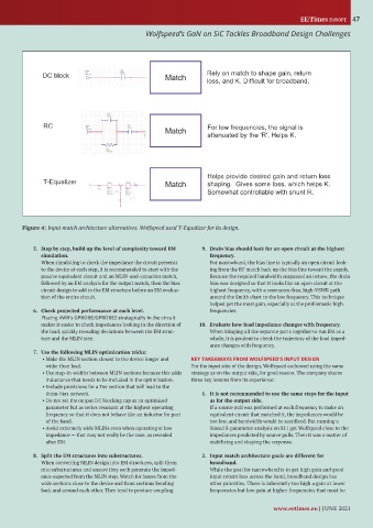
           Figure 4: Input match architecture alternatives. Wolfspeed used T-Equalizer for its design.


               5.   Step by step, build up the level of complexity toward EM     9.   Drain bias should look for an open circuit at the highest
                 simulation.                                           frequency.
                 When simulating to check the impedance the circuit presents   For narrowband, the bias line is typically an open circuit look-
                 to the device at each step, it is recommended to start with the   ing from the RF match back up the bias line toward the supply.
                 passive equivalent circuit and an MLIN-and-capacitor match,   Because the required bandwidth surpassed an octave, the drain
                 followed by an EM analysis for the output match, then the bias   bias was designed so that it looks like an open circuit at the
                 circuit design to add to the EM structure before an EM evalua-  highest frequency, with a resonance-free, high-VSWR path
                 tion of the entire circuit.                           around the Smith chart to the low frequency. This technique
                                                                       helped get the most gain, especially at the problematic high
               6.  Check projected performance at each level.          frequencies.
                 Placing AWR’s GPROBE/GPROBE2 strategically in the circuit
                 makes it easier to check impedances looking in the direction of     10.  Evaluate how load impedance changes with frequency.
                 the load, quickly revealing deviations between the EM struc-  When bringing all the separate parts together to run EM as a
                 ture and the MLIN step.                               whole, it is prudent to check the trajectory of the load imped-
                                                                       ance changes with frequency.
               7.  Use the following MLIN optimization tricks:
                  •  Make the MLIN section closest to the device longer and   KEY TAKEAWAYS FROM WOLFSPEED’S INPUT DESIGN
                   wider than lead.                              For the input side of the design, Wolfspeed eschewed using the same
                  •  Use step-in-widths between MLIN sections because this adds   strategy as on the output side, for good reason. The company shares
                   inductance that needs to be included in the optimization.  three key lessons from its experience:
                  •  Include provisions for a Tee section that will lead to the
                   drain-bias network.                               1.   It is not recommended to use the same steps for the input
                  •  Do not set the output DC blocking cap as an optimized   as for the output side.
                   parameter but as series resonant at the highest operating   If a source pull was performed at each frequency to make an
                   frequency so that it does not behave like an inductor for part   equivalent circuit that matched it, the impedances would be
                   of the band.                                        too low, and bandwidth would be sacrificed. But running a
                  •  Avoid extremely wide MLINs even when operating at low   biased S-parameter analysis on S11 got Wolfspeed close to the
                   impedance — that may not really be the case, as revealed   impedances predicted by source pulls. Then it was a matter of
                   after EM.                                           stabilizing and shaping the response.

               8.  Split the EM structures into substructures.       2.   Input match architecture goals are different for
                 When converting MLIN design into EM structures, split them   broadband.
                 into substructures and ensure they each generate the imped-  While the goal for narrowband is to get high gain and good
                 ance expected from the MLIN step. Watch for issues from the   input return loss across the band, broadband design has
                 wide sections close to the device and from sections bending   other priorities. There is inherently too high a gain at lower
                 back and around each other. They tend to produce coupling.  frequencies but low gain at higher frequencies that must be

                                                                                           www.eetimes.eu | JUNE 2021

