Page 46 - EETimes Europe June 2021
P. 46
46 EE|Times EUROPE

           Wolfspeed’s GaN on SiC Tackles Broadband Design Challenges


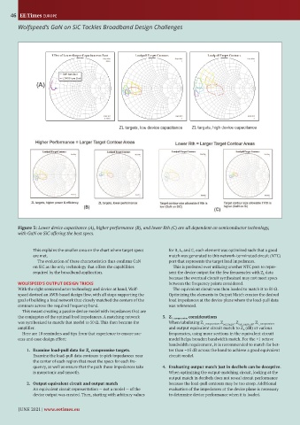
           Figure 3: Lower device capacitance (A), higher performance (B), and lower Rth (C) are all dependent on semiconductor technology,
           with GaN on SiC offering the best specs.


                 This explains the smaller area on the chart where target specs   for R, L, and C, each element was optimized such that a good
                 are met.                                              match was generated to this network-terminated circuit (NTC)
                   The evaluation of these characteristics thus confirms GaN   port that represents the target load impedances.
                 on SiC as the only technology that offers the capabilities   This is preferred over utilizing another NTC port to repre-
                 required by the broadband application.                sent the device output for the few frequencies with Z L  data
                                                                       because the eventual circuit synthesized may not meet specs
           WOLFSPEED’S OUTPUT DESIGN TRICKS                            between the frequency points considered.
           With the right semiconductor technology and device at hand, Wolf-  The equivalent circuit was then loaded to match it to 50 Ω.
           speed devised an AWR-based design flow, with all steps supporting the   Optimizing the elements in Output Match creates the desired
           goal of building a load network that closely matched the centers of the   load impedances at the device plane where the load-pull data
           contours across the required frequency band.                was referenced.
             This meant creating a passive device model with impedances that are
           the conjugates of the optimal load impedances. A matching network     3.  Z L_compromise  considerations
           was synthesized to match that model to 50 Ω. This then became the   When tabulating Z L_compromise , Z out_target , Z out_equiv_ckt , Z L_compromise ,
           amplifier.                                                  and output equivalent circuit match to Z L  (dB) at various
             Here are 10 reminders and tips from that experience to ensure suc-  frequencies, using more sections in the equivalent circuit
           cess and ease design effort:                                model helps broaden bandwidth match. For the >1 octave
                                                                       bandwidth requirement, it is recommended to match for bet-
               1.  Examine load-pull data for Z L  compromise targets.  ter than –15 dB across the band to achieve a good equivalent
                 Examine the load-pull data contours to pick impedances near   circuit model.
                 the center of each region that meet the specs for each fre-
                 quency, as well as ensure that the path these impedances take     4.   Evaluating output match just in decibels can be deceptive.
                 is monotonic and smooth.                              When optimizing the output-matching circuit, looking at the
                                                                       output match in decibels does not reveal circuit performance
               2.  Output equivalent circuit and output match          because the load-pull contours may be too steep. Additional
                 An equivalent circuit representation — not a model — of the   evaluation of the impedances at the device plane is necessary
                 device output was created. Then, starting with arbitrary values   to determine device performance when it is loaded.

           JUNE 2021 | www.eetimes.eu

