Page 45 - EETimes Europe June 2021
P. 45
EE|Times EUROPE   45

                                                  Wolfspeed’s GaN on SiC Tackles Broadband Design Challenges


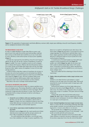
           Figure 2: The separation of output power and drain efficiency contours (left), target specs defining a locus for each frequency (middle),
           and an unaligned movement of loci (right)


           THE BROADBAND CHALLENGE                                     faster turn-on and turn-off and lower gate drive losses. The
           It would be wishful thinking to assume that efficiency, power, and   Smith chart in Figure 3a, left, shows a representation of device
           gain all reach their peak values at the same load impedance and that   output impedance for LDMOS (pink) and GaN (blue). GaN’s
           their contours on the Smith chart would line up on top of each other.   lower output capacitance and the smaller package parasitics
           In reality, efficiency comes at the expense of output power capability   delivered by Wolfspeed help the output impedances to stay
           (Figure 2).                                                 confined against frequency.
             Consider the target specifications defining a locus for each frequency   An examination of the load impedance or load-pull target
           wherein all the specs are met for a region of impedances, as shown in   contours and loci of representative GaN (Figure 3a,
           Figure 2, middle. This locus of compliance moves as well as changes   middle) and LDMOS (Figure 3a, right) devices shows that
           size and shape with frequency. Whereas the lower frequencies tend to   GaN’s contours and movement align better. GaN’s “green
           have wider regions on the Smith chart where specs are met, the higher   arrow” of movement would be shorter, flatter, and therefore
           frequencies have tighter regions of compliance because of device and   easier to match than that of an LDMOS device, with its green
           package parasitics.                                         arrow a sharper curve.
             Another problem is that these regions of compliance do not move in   This clearly makes GaN the technology of choice for broad-
           the same way as the load impedance, as the microstrip lines (MLINs)   band design.
           and shunt capacitances used for impedance matching rotate differently
           with frequency (Figure 2, right). The load impedance (blue arrow)     3.   Higher inherent performance makes target contour areas
           tends to move clockwise with frequency, while target impedances   larger.
           (green arrow) tend to move counterclockwise as well as disperse.  Consider a case where the load-pull contours at a given
             This, then, is the major challenge with broadband design.  frequency trace out large areas of the Smith chart. This would
                                                                       mean that the circuit would more easily hit target specs with
           GaN ON SiC ADDRESSES CHALLENGES                             varying frequency.
           Several factors can be used to better align the contours and their move-  Such generous contours come from higher inherent per-
           ments for design success. The strategy should be to make the target and   formance of the device itself (Figure 3b, left) — in this case,
           circuit impedances flatter and to make the contour loci bigger, offering   GaN on SiC. The contours have a high peak value and change
           a generous-enough area when the design is in spec. This in-spec area   slowly with changes in impedance. That green arrow of change
           is dependent both on design techniques and device technology, as   is flattened.
           discussed below:                                              Contrast this against the plot for lower performance
                                                                       (Figure 3b, right), which is slightly exaggerated to illustrate
               1.  Circuit ZL curve is flatter with more matching sections.  the point. Lower-performance circuits have difficulty hitting
                 The blue curve for the circuit impedances, shown earlier in   the target specs at all frequencies.
                 Figure 2, is flatter when more matching sections are used. This
                 means fully utilizing transmission lines, with careful changes     4.  Lower thermal impedance increases target contour areas.
                 in lengths and widths, as well as shunt capacitors.   There is a reason why SiC is the leading technology when high
                                                                       power density is needed: its exceptional thermal conductivity.
               2.   Lower device capacitances make broadband circuit match-  Against Si’s 1.5 W/cm⋅K, SiC offers 3.3–4.5 W/cm⋅K.
                 ing easier.                                             The two Smith charts in Figure 3c put this advantage in
                 The green curve in Figure 2 for the target impedances is flatter   perspective by comparing two types of GaN technology — GaN
                 when the device capacitance and the package parasitics are   on SiC on the left and GaN on Si on the right.
                 lower. This is dependent on the device technology.      The higher thermal impedance of GaN on Si means that
                   It is well-established that GaN offers a very low gate capac-  higher efficiency is needed at any given output power to keep
                 itance that contributes to its high-frequency capabilities, with   the junction temperature lower than the selected threshold.

                                                                                           www.eetimes.eu | JUNE 2021

