
Page 32 - PEN eBook May 2023
P. 32
SEMICONDUCTORS SEMICONDUCTORS
FIT rates have been calculated for both data HOT CARRIER DEGRADATION
center/server and telecom mission-specific usage Hot carriers generated through current flow at high
profiles. As the table in Figure 2 shows, excellent FIT voltages can cause both charge trapping (resulting in
rates of well below 1 are seen from these TDB stress dynamic R DS(on) increases) and create device
conditions. wear-out due to defect generation. The JEP-180
guideline enables a switching lifetime to be determined
CHARGE TRAPPING
Charge trapping is an occurrence wherein “traps”
in the semiconductor material cause charge to stop,
causing a momentary increase in resistance at the
time of a FET turning on. After a small amount of time,
measured in nanoseconds, the traps are full and the
FET operates as expected. When the FET is turned off,
Figure 1: Reliability testing standards and guidelines used for these traps are released. A result of this trapping is
power GaN (Source: Texas Instruments)
typically an increase in the device’s on-state resistance
(R DS(on) ), as negatively charged traps repel the channel
TESTING STANDARDS AND electrons. This increase is called dynamic R
DS(on)
GUIDELINES degradation, as some of this trapping can be reversible
As shown in Figure 1, GaN reliability testing can be and can also depend on the aging of the device.
categorized into component and power supply levels. Charge trapping can occur in GaN HEMT devices in the
Parts are qualified both under the buffer layer under the channel, in the dielectrics or at
silicon-device–developed standards, such as AEC-Q100, the device layer interfaces. It can occur under static
but additionally tested for GaN-specific failure conditions with a high drain bias or under dynamic
mechanisms covered under the JEP-180, JEP-173 and switching conditions.
JEP-182 JEDEC guidelines. Power-supply–level testing
is focused on real-world situations and the impact to
the GaN FET, which involves running
application-specific tests for robustness from
occasional events, such as power surges and
short-circuits.
Let’s look at some of the GaN-specific tests in more
detail.
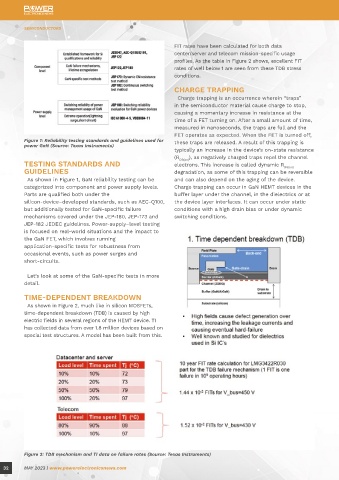
TIME-DEPENDENT BREAKDOWN
As shown in Figure 2, much like in silicon MOSFETs, Figure 3: GaN charge trapping mechanism and dynamic R DS(on)
time-dependent breakdown (TDB) is caused by high measurements from TI (Source: Texas Instruments)
electric fields in several regions of the HEMT device. TI
has collected data from over 1.8 million devices based on Low-duty–cycle, hard-switch testing can provide
special test structures. A model has been built from this. higher sensitivity for dynamic R DS(on) degradation. As
shown in Figure 3, TI uses a test vehicle listed in the
JEP-182 standard to provide a continuous
hard-switching stress based on the maximum power
condition, the maximum recommended drain voltage
(V ) and the worst-case junction temperature. These
DS
conditions are per the JEP-180 guidelines.
The data over 1,000 hours of stress testing at a
duty cycle of 0.5% is shown in Figure 3. This shows
a stable R DS(on) behavior with device aging. A static
off-state stress of 500-V V at 125°C on the LMG341x
DS
GaN product similarly shows no R DS(on) degradation.
This stable R DS(on) behavior in TI’s GaN devices comes
from many years of process flow improvements in key Figure 4: The DHTOL guideline of JEP-180 validates reliability
process steps like epi-growth as well as creating for stresses of the relevant target application (Source: Texas
Figure 2: TDB mechanism and TI data on failure rates (Source: Texas Instruments) trap-free dielectrics and interfaces. Instruments)
32 MAY 2023 | www.powerelectronicsnews.com MAY 2023 | www.powerelectronicsnews.com 33