
Page 13 - PEN eBook July 2023
P. 13
Cover Story — Design
The derating of the LDO sets in right from the start. Due to the working principle of the LDO, the
losses are too much at a ratio of V = 24 V to V = 5 V. This means it can deliver only 0.1 A, although
IN OUT
it is rated for 1 A. In contrast to the power module, there will always be a need for additional means
of cooling, which must be provided to allow the proper operation of an LDO for higher ratios of V
IN
to V .
OUT
In contrast, the VDLM 171013801 has no derating up to 105°C with an output current of 1 A for
V = 24 V to V = 5 V, meaning the solution size, weight and cost are much lower compared with
IN OUT
a solution based on an LDO.
Over 90% of the power that is put
into the 171013801 will be used
for supplying the application. In
comparison, the LDO uses only 20%
of the input power for this task,
while the remaining 80% of the
power will be converted into heat
that has to be dissipated by the
LDO.
Operation under low efficiency
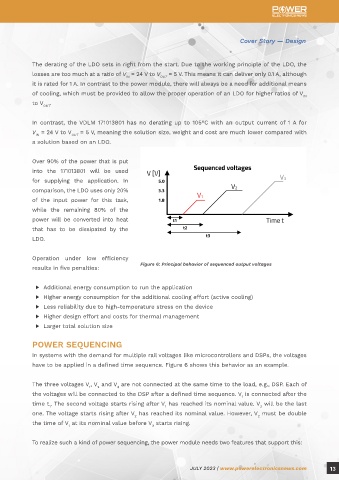
Figure 6: Principal behavior of sequenced output voltages
results in five penalties:
▶ Additional energy consumption to run the application
▶ Higher energy consumption for the additional cooling effort (active cooling)
▶ Less reliability due to high-temperature stress on the device
▶ Higher design effort and costs for thermal management
▶ Larger total solution size
POWER SEQUENCING
In systems with the demand for multiple rail voltages like microcontrollers and DSPs, the voltages
have to be applied in a defined time sequence. Figure 6 shows this behavior as an example.
The three voltages V , V and V are not connected at the same time to the load, e.g., DSP. Each of
1 2 3
the voltages will be connected to the DSP after a defined time sequence. V is connected after the
1
time t . The second voltage starts rising after V has reached its nominal value. V will be the last
1 1 3
one. The voltage starts rising after V has reached its nominal value. However, V must be double
2 2
the time of V at its nominal value before V starts rising.
1 3
To realize such a kind of power sequencing, the power module needs two features that support this:
JULY 2023 | www.powerelectronicsnews.com 13