
Page 27 - PEN eBook NOVEMBER 2022
P. 27
SEMICONDUCTORS SEMICONDUCTORS
conduction and switching losses affect the overall
efficiency. In hard switching, turn-on losses can
dominate due to reverse recovery and junction
capacitance charge. The loss from input gate
capacitance switching-node charge/discharge also has
a major role at high frequencies. The high di/dt and
dV/dt from high-frequency HS also place
third-quadrant hard-commutation requirements on the
device, which can be another loss component. Within
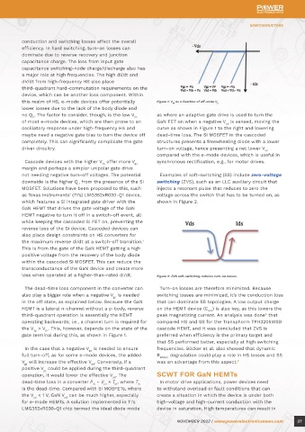
this realm of HS, e-mode devices offer potentially Figure 1: V sd as a function of off-state V g
lower losses due to the lack of the body diode and
no Q . The factor to consider, though, is the low V as where an adaptive gate drive is used to turn the
rr
th
of most e-mode devices, which are then prone to an GaN FET on when a negative V is sensed, moving the
ds
oscillatory response under high-frequency HS and curve as shown in Figure 1 to the right and lowering
maybe need a negative gate bias to turn the device off dead-time loss. The Si MOSFET in the cascoded
completely. This can significantly complicate the gate structures presents a freewheeling diode with a lower
driver circuitry. turn-on voltage, hence presenting a net lower V
sd
compared with the e-mode devices, which is useful in
GaN HEMTs: Device margin and perhaps a simpler unipolar gate drive gs synchronous rectification, e.g., for motor drives.
Cascode devices with the higher V offer more V
th
Examples of soft-switching (SS) include zero-voltage
Characteristics and not needing negative turn-off voltages. The potential switching (ZVS), such as an LLC auxiliary circuit that
downside is the higher Q from the presence of the Si
rr
injects a resonant pulse that reduces to zero the
MOSFET. Solutions have been proposed to this, such
Application Tradeoffs as Texas Instruments’ (TI’s) LMG352xR030-Q1 device, voltage across the switch that has to be turned on, as
shown in Figure 2.
which features a Si integrated gate driver with the
GaN HEMT that drives the gate voltage of the GaN
HEMT negative to turn it off in a switch-off event, all
By Sonu Daryanani, contributing writer for Power Electronics News while keeping the cascoded Si FET on, preventing the
reverse loss of the Si device. Cascoded devices can
also place design constraints on HS converters for
Gallium nitride HEMT devices are at the forefront achieved, and Transphorm, Nexperia, and others the maximum reverse di/dt at a switch-off transition.
1
of creating new opportunities as well as replacing offer some examples of this. This is from the gate of the GaN HEMT getting a high
existing silicon-based designs in a wide range of positive voltage from the recovery of the body diode
power-conversion and power-delivery applications. E-mode devices have the advantage of using some within the cascoded Si MOSFET. This can reduce the
In this article, we will review some of the key device of the intrinsic benefits of the GaN HEMT, such as no transconductance of the GaN device and create more
characteristics of some of the more widely available reverse-recovery loss due to lack of a p-n junction in loss when operated at a higher-than-rated di/dt. Figure 2: ZVS soft-switching reduces turn-on losses.
HEMTs and try to highlight some of the tradeoffs on the drain/source, as well as simpler/lower parasitics
each one. from not having an additional device in series. One big The dead-time loss component in the converter can Turn-on losses are therefore minimized. Because
disadvantage, however, is the poor margin for gate drive also play a bigger role when a negative V is needed switching losses are minimized, it’s the conduction loss
gs
The two most widely used approaches to GaN HEMTs and a susceptibility to gate noise from the low V . in the off state, as explained below. Because the GaN that can dominate SS topologies. A low output charge
th
for power applications are: HEMT is a lateral n-channel without a p-body, reverse on the HEMT device (C ) is also key, as this lowers the
oss
The cascode approach solves the poor gate margin third-quadrant operation is essentially the HEMT peak magnetizing current. An analysis was done that
2
▶ The e-mode approach, where the device of the e-mode and offers a more robust gate. This, operating backwards; i.e., a channel turn is required for compared HS and SS for the Transphorm TPH3205WSB
could be formed with a p-GaN Schottky gate however, is at the expense of potentially having higher the V > V . This, however, depends on the state of the cascode HEMT, and it was concluded that ZVS is
dg
th
and result in a V of about 1.7 V. Examples of switching losses from reverse recovery (Q ) in the Si FET. gate terminal during this, as shown in Figure 1. preferred when efficiency is the primary target and
rr
t
this approach would be devices offered by Approaches taken to mitigate this are discussed later. that SS performed better, especially at high switching
GaN Systems, GaN Power International, and In the case that a negative V is needed to ensure frequencies. Böcker et al. also showed that dynamic
gs
Innoscience, to name just a few. A notable Some important application performance examples full turn-off, as for some e-mode devices, the added R DS(on) degradation could play a role in HS losses and SS
exception to the relatively low V for e-mode are listed below and a comparison is made between V will increase the effective V . Conversely, if a was an advantage from this aspect. 3
t
sd
gs
devices is the offering from Cambridge GaN the two device approaches listed above. positive V could be applied during the third-quadrant
gs
Devices, which offers >2-V e-mode devices operation, it would lower the effective V . The SCWT FOR GaN HEMTs
sd
through some innovative design approaches. HARD-/SOFT-SWITCHING dead-time loss in a converter P ~ V × T , where T In motor drive applications, power devices need
dt
dt
sd
dt
CHARACTERISTICS OF GaN HEMTs is the dead-time. Compared with Si MOSFETs, where to withstand overload or fault conditions that can
▶ The cascode approach, where a low-voltage Examples of hard switching (HS) include synchronous the V < 1 V, GaN V can be much higher, especially create a situation in which the device is under both
sd
sd
Si MOSFET is essentially placed in series buck/boost converters and continuous-conduction– for e-mode HEMTs. A solution implemented in TI’s high-voltage and high-current conduction with the
and creates the gate drive. Higher V can be mode totem-pole PFC AC/DC converters. Both LMG352xR030-Q1 chip termed the ideal diode mode device in saturation. High temperatures can result in
t
36 NOVEMBER 2022 | www.powerelectronicsnews.com NOVEMBER 2022 | www.powerelectronicsnews.com 37