Page 22 - PEN eBook NOVEMBER 2022
P. 22
DESIGN DESIGN
Figure 2: Thermally optimized MPQ4323 schematic that meets automotive EMC
The recommended layout has a solid top, bottom GND
A Thermally Optimized, THE METHOD plane, and a large V polygon. It also utilizes P GND vias
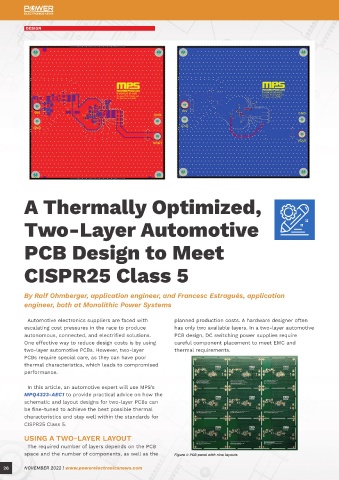
For this article, we tested nine two-layer layouts.
IN
to connect the top and bottom layer. Figure 4 shows
Each layout had unique component positions and slight
Two-Layer Automotive modifications compared with the other PCBs, as well the solution’s thermal image. The Y-shaped V heatsink
IN
polygon extracts heat on the top layer. P
as different placements for the polygons and vias (see
vias are
GND
Figure 1). The purpose of using nine layouts was to find
connected to the top and bottom layers to act as a
PCB Design to Meet a successful solution with improved EMC and thermals. second effective heatsink.
This article will focus on the differences between the
thermal and EMC performances between these layouts.
CISPR25 Class 5 RECOMMENDATIONS FOR A TWO-
LAYER LAYOUT
By following certain design rules, it is possible
to achieve a solution that has been optimized for
By Ralf Ohmberger, application engineer, and Francesc Estragués, application thermals and EMC. Figure 2 shows an example of
engineer, both at Monolithic Power Systems a circuit using MPS’s MPQ4323-AEC1, a DC power
switching supply that meets automotive EMC CISPR25
Automotive electronics suppliers are faced with planned production costs. A hardware designer often Class 5 requirements while using a thermally optimized
escalating cost pressures in the race to produce has only two available layers. In a two-layer automotive two-layer layout.
autonomous, connected, and electrified solutions. PCB design, DC switching power supplies require
One effective way to reduce design costs is by using careful component placement to meet EMC and Figure 3 shows the PCB component placement using
two-layer automotive PCBs. However, two-layer thermal requirements. the schematic from Figure 2. Figure 4: MPQ4323 two-layer PCB thermal image
PCBs require special care, as they can have poor
thermal characteristics, which leads to compromised The inductor (L3) acts as effective heatsink (see
performance. Figure 4). In this example, the switching node on pin
12 must have a small surface area so that it does not
In this article, an automotive expert will use MPS’s act as an emmitting antenna due to its fast-changing
MPQ4323-AEC1 to provide practical advice on how the voltage (high dU/dt). Place the inductor as close as
schematic and layout designs for two-layer PCBs can possible to pin 12, as the short distance allows for
be fine-tuned to achieve the best possible thermal optimal heat flow into the inductor. For excellent EMC,
characteristics and stay well within the standards for place the marked side of the inductor winding so
CISPR25 Class 5. that it aligns with pin 12. This allows the outer copper
windings of the inductance to shield the inductor
USING A TWO-LAYER LAYOUT coil’s noisy inner area, which has a high dU/dt. Figure 5
The required number of layers depends on the PCB shows the heat distribution in the package.
space and the number of components, as well as the Figure 1: PCB panel with nine layouts Figure 3: MPQ4323 two-layer PCB component placement
26 NOVEMBER 2022 | www.powerelectronicsnews.com NOVEMBER 2022 | www.powerelectronicsnews.com 27

