
Page 15 - PEN eBook NOVEMBER 2022
P. 15
DESIGN DESIGN
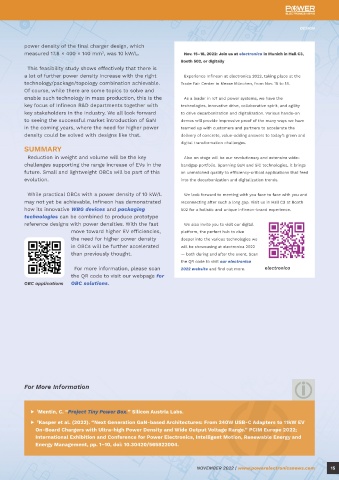
different power semiconductor technologies are used power density of the final charger design, which
in the same design (Figure 5). measured 17.8 × 400 × 140 mm , was 10 kW/L. Nov. 15–18, 2022: Join us at electronica in Munich in Hall C3,
3
Booth 502, or digitally
MOSFET packages can be thermally bonded to a cold This feasibility study shows effectively that there is
plate in several ways. Still, the most straightforward a lot of further power density increase with the right Experience Infineon at electronica 2022, taking place at the
and most effective approach is to place a single technology/package/topology combination achievable. Trade Fair Center in Messe München, from Nov. 15 to 18.
thermally conductive gap filler between a MOSFET and Of course, while there are some topics to solve and
its heatsink. This approach also has the advantage enable such technology in mass production, this is the As a leader in IoT and power systems, we have the
of allowing the production process to be fully key focus of Infineon R&D departments together with technologies, innovative drive, collaborative spirit, and agility
automated. While the gap filler can provide sufficient key stakeholders in the industry. We all look forward to drive decarbonization and digitalization. Various hands-on
electrical isolation, for extra safety, an additional to seeing the successful market introduction of GaN demos will provide impressive proof of the many ways we have
isolation foil can be used to provide further electrical in the coming years, where the need for higher power teamed up with customers and partners to accelerate the
isolation without significant deterioration in thermal density could be solved with designs like that. delivery of concrete, value-adding answers to today’s green and
performance. digital transformation challenges.
SUMMARY
HOW TO ADDRESS OBC POWER Reduction in weight and volume will be the key Also on stage will be our revolutionary and extensive wide-
DENSITY EVOLUTION challenges supporting the range increase of EVs in the bandgap portfolio. Spanning GaN and SiC technologies, it brings
Infineon collaborated with Silicon Austria Labs to future. Small and lightweight OBCs will be part of this an unmatched quality to efficiency-critical applications that feed
develop a 7-kW automotive OBC design to demonstrate evolution. into the decarbonization and digitalization trends.
high power density utilizing SiC and TSC package
innovation. While practical OBCs with a power density of 10 kW/L We look forward to meeting with you face to face with you and
may not yet be achievable, Infineon has demonstrated reconnecting after such a long gap. Visit us in Hall C3 at Booth
This is a single-phase, isolated, bidirectional charger how its innovative WBG devices and packaging 502 for a holistic and unique Infineon-brand experience.
Figure 6: Tiny Power Box OBC developed collaboratively by with an integrated low-voltage 2.4-kW, 12-V output. technologies can be combined to produce prototype
Silicon Austria Labs, Infineon, and other partners The reference design, which occupies a volume of reference designs with power densities. With the fast We also invite you to visit our digital
about 3.2 kW/L (including the case and connectors), move toward higher EV efficiencies, platform, the perfect hub to dive
and they also have a Kelvin source pin to control uses Infineon’s TSC 750-V SiC MOSFETs to achieve an the need for higher power density deeper into the various technologies we
*
efficiency (Figure 4). overall peak efficiency of about 97%, including the PFC in OBCs will be further accelerated will be showcasing at electronica 2022
and C LLC converters (Figure 6). 1 than previously thought. — both during and after the event. Scan
ASSEMBLY CONSIDERATIONS the QR code to visit our electronica
Heat-generating MOSFET devices and heatsinks are Toward an even high-power–density class, Infineon For more information, please scan 2022 website and find out more. electronica
generally placed on the top side of a PCB alongside collaborated with the Power Electronic Systems the QR code to visit our webpage for
other low-profile components. In contrast, taller Laboratory, ETH Zürich, on a super-high–density OBC OBC applications OBC solutions.
devices are typically placed on the underside of the design based on GaN HEMT technology. 2
board. Infineon’s HDSOP devices are designed to have
a uniform height of 2.3 mm, simplifying cold plate By combining advanced control and modulation
attachment and removing the need for machining. This schemes with the superior behavior of these devices
also allows optimized heatsinks to be used, even where under different switching conditions, the uncased
For More Information
▶ Mentin, C. “Project Tiny Power Box.” Silicon Austria Labs.
1
▶ Kasper et al. (2022). “Next Generation GaN-based Architectures: From 240W USB-C Adapters to 11kW EV
2
On-Board Chargers with Ultra-high Power Density and Wide Output Voltage Range.” PCIM Europe 2022;
Figure 7: GaN HEMT-based OBC designed by ETH Zurich and Infineon International Exhibition and Conference for Power Electronics, Intelligent Motion, Renewable Energy and
Energy Management, pp. 1–10, doi: 10.30420/565822004.
* Coming soon. For product availability or sample requests contact our support
14 NOVEMBER 2022 | www.powerelectronicsnews.com NOVEMBER 2022 | www.powerelectronicsnews.com 15