
Page 11 - PEN eBook NOVEMBER 2022
P. 11
DESIGN DESIGN
Signposting a
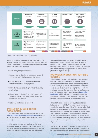
Roadmap Toward Figure 1: Key challenges facing OBC designers
Higher-Power–Density When not used, it is transported around within the topologies to increase the power density in active
vehicle, its size and weight negatively impacting vehicle
devices and reduce passive components, such as
inductors and capacitors. Also, the wide voltage
range. There are six critical and interrelated challenges
EV OBCs facing OBC designers (Figure 1): offering here is important, which enables the coverage
of different battery voltages and also native three-
phase topologies in design.
Need for higher-power classes
▶
Key challenges, impactful innovations, and WBG solution ▶ Increase power density to reduce the size and PACKAGING INNOVATION: TOP-SIDE
COOLING
weight of the EV OBC to extend the range
The heat-conduction path for high-power surface-
enablers for major OBC trends ▶ Maximize efficiency to enable higher power mounted electronic devices is usually vertically
density and reduce charging time downward from the component toward the printed-
By Daniel Makus, global application manager for xEV and EV charging at Infineon circuit board (PCB), which is bonded to a cold plate
Technologies; Christian Mentin, senior scientist at Silicon Austria Labs; and Rafael ▶ Bidirectional operation to provide grid stability — so-called “bottom-side cooling” (BSC) — but this
A. Garcia Mora, system application engineer for OBC applications at Infineon and backup creates a compromise between thermal performance
Technologies ▶ Rising battery voltages (from 400 V to 800 V) and PCB usage. Infineon has developed innovative
packaging, which allows discrete semiconductors
to reduce current and associated heating on and power ICs to be top-side–cooled (TSC) and also
The highly dynamic nature of the automotive industry novel circuit topologies and innovations in packaging cables and connectors delivers additional benefits in the design of OBCs.
means that designers of on-board chargers (OBCs) on-board assemblies.
for electric vehicles are faced with a set of goalposts ▶ Balancing performance and cost With BSC, a cold plate is usually attached to the
that are constantly moving, as regulations relating In this article, Infineon takes stock of the immediate bottom side of the PCB. This prevents components
to efficiency and grid integration are continuously challenges facing OBC designers and discusses changes from being placed on one side of the board, effectively
reviewed and updated. in how they are using WBG devices. It also considers EVOLUTION IN WBG DEVICE halving the attainable power density. Semiconductor
how thermally managed device packaging and assembly TOPOLOGIES devices are thermally bonded to the PCB, which means
To stay ahead of the game, designers are now techniques can help significantly improve OBC power Designers are already successfully exploiting the they function at the same temperature as the board.
pursuing ambitious targets, such as increasing the density before presenting two reference designs that superior capabilities of WBG technologies to meet As the maximum operating temperature of a PCB (Tg)
importance of high-power–density levels of OBCs. If push the boundaries of currently attainable levels of these challenges, but how they use them is still is lower than the operating temperature of most power
the state-of-the-art density was less than 2 kW/L power density and can provide pointers for how even evolving. devices, their advantages cannot be fully exploited
yesterday, current designs are going toward 4 kW/L higher levels will be realized in the future. (Figure 2).
and suppose to increase to more than 6 kW/L by the Higher-power classes are leading to changing
end of the decade. Charting a course toward achieving OBCs: DESIGN CHALLENGES topologies and how solutions are implemented. For With TSC, a cold plate is bonded to the top side of
this figure over the longer term will be multi-faceted, The role of the OBC in an EV is to convert AC grid example, designers are increasingly moving toward the power components, thus allowing components to
requiring wide-bandgap (WBG) semiconductors in power into a DC voltage to charge the traction battery. active and efficient rectifiers and fast-switching be placed on both sides of the PCB and enabling WBG
10 NOVEMBER 2022 | www.powerelectronicsnews.com NOVEMBER 2022 | www.powerelectronicsnews.com 11