
Page 12 - PEN eBook NOVEMBER 2022
P. 12
DESIGN DESIGN
Figure 2: The innovative top-side–cooling concept permits double-sided component placement and allows for a doubling of
power density.
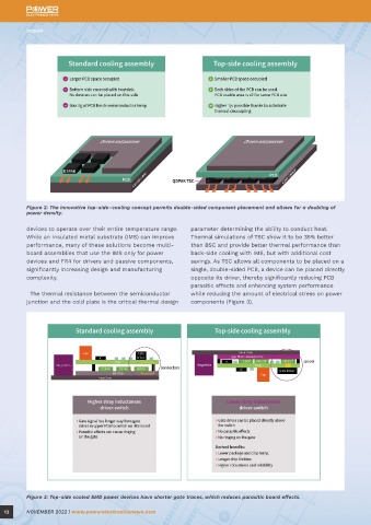
devices to operate over their entire temperature range. parameter determining the ability to conduct heat.
While an insulated metal substrate (IMS) can improve Thermal simulations of TSC show it to be 35% better
performance, many of these solutions become multi- than BSC and provide better thermal performance than
board assemblies that use the IMS only for power back-side cooling with IMS, but with additional cost
devices and FR4 for drivers and passive components, savings. As TSC allows all components to be placed on a
significantly increasing design and manufacturing single, double-sided PCB, a device can be placed directly Figure 4: The TSC-capable QDPAK provides several benefits for packaging and assembly.
complexity. opposite its driver, thereby significantly reducing PCB
parasitic effects and enhancing system performance Infineon’s QDPAK devices are designed to take QDPAK devices can dissipate large amounts of power
The thermal resistance between the semiconductor while reducing the amount of electrical stress on power advantage of the benefits of TSC, and these offer up to 35 W (depending on the thermal interfaces
junction and the cold plate is the critical thermal design components (Figure 3). several features that make them suitable for use in and entire cooling system) and have multiple pins
various applications. They also offer easy assembly dedicated to the drain and source connections,
with a nominal footprint of 20.96 × 15.00 mm and a making them ideal for high-current applications.
consistent 2.3-mm height throughout the series. Their symmetrical, parallel lead layout also ensures
mechanical stability and easy assembly and testing,
Figure 3: Top-side cooled SMD power devices have shorter gate traces, which reduces parasitic board effects. Figure 5: HDSOP devices simplify the design and assembly of the heatsink.
12 NOVEMBER 2022 | www.powerelectronicsnews.com NOVEMBER 2022 | www.powerelectronicsnews.com 13