
Page 25 - PEN Ebook March 2021
P. 25
Design Design
Equation (7)). Note that both the angle/phase and phase boost at the BW frequency. In theory, the
the slope/magnitude due to a pole/zero will start positive phase due to a zero reaches its maxi-
changing at 10% of the pole/zero frequency and mum value at 10 times its frequency. Therefore,
will reach their maximum value at 10 times the set COMP-Z between 10% and 20% of the BW
frequency of the pole/zero. frequency. The range accounts for any additional
parasitic effects in the system. Therefore, the
The frequency of COMP-Z can be calculated with relation between the COMP-Z frequency and the
Equation (6): BW frequency can be calculated with Equation (9):
(6) (9)
The frequency of COMP-P can be calculated with For proper noise attenuation at higher frequen-
Equation (7): cies, the pole by the compensator (COMP-P)
must be approximately equal to f / 2, assum-
SW
(7) ing that the switching frequency is <1MHz. If the
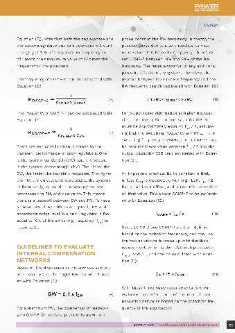
Figure 1: PCM Buck Regulator Schematic and Bode Plot. switching frequency is >1MHz, then COMP-P must
PEAK CURRENT MODE BUCK The ESR zero frequency in PCM-controlled buck There are two criteria when it comes to the be near the lower value between f / 2 and the
SW
REGULATORS regulators (ω ) can be calculated with Equation (5): transient performance of buck regulators. One output capacitor ESR zero, estimated with Equa-
Z
Peak current mode (PCM) control is widely used as is the system bandwidth (BW), and the second tion (5).
the control method for buck regulators. The bene- (5) is the system phase margin (PM). The higher the
fits associated with PCM control over voltage mode BW, the faster the transient response. The higher An important practical tip to consider is that,
(VM) control have already been well established. TYPICAL TYPE II COMPENSATION the PM, the quieter and more stable the system. unless C OUT is electrolytic with high ESR, f / 2
SW
Figure 1 shows the application schematic and typi- NETWORK Unfortunately, in practice, increasing the BW has a dominant effect, and COMP-P is dependent
cal bode diagram for a PCM buck regulator. Figure 2 shows a typical Type II compensation decreases the PM, and vice versa. This means on that value. This allows COMP-P to be estimat-
network. A Type II compensation adds one zero there is a tradeoff between BW and PM. To have ed with Equation (10):
The two power-stage pole frequencies in Figure 1 (COMP-Z) and one pole (COMP-P) to a system. a proper BW along with an acceptable PM and
can be calculated with Equation (1) and Equation The frequency of COMP-Z and COMP-P can be acceptable noise level in a buck regulator, a BW (10)
(2), respectively: calculated based on the passive components equal to 10% of the switching frequency (f ) is
SW
of the system (see Figure 2, Equation (6), and reasonable. Since COMP-Z and COMP-P are both defined
based on the switching frequency, one can use
(1) the two equations to come up with the third
GUIDELINES TO EVALUATE requirement, which is the relationship between
INTERNAL COMPENSATION C COMP and C , and can be calculated with Equa-
HF
(2) NETWORKS tion (11):
Based on the discussion in the previous section,
Where R can be calculated with Equation (3): let’s assume that the target BW can be calculat- (11)
i
ed with Equation (8):
(3) With these three basic requirements, one can
(8) evaluate the performance of the internal com-
And K can be calculated with Equation (4), when pensation networks based on the switching fre-
m
D = 0.5 (D represents the duty cycle): For a maximum PM, the compensation network quency of the application.
Figure 2: Type II Compensation Network and Zero/Pole
Locations. zero (COMP-Z) needs to provide its maximum
(4)
24 MARCH 2021 | www.powerelectronicsnews.com MARCH 2021 | www.powerelectronicsnews.com 25