
Page 21 - PEN Ebook March 2021
P. 21
Semiconductors Semiconductors
needed to properly turn the transistor off. There THE IMPACT OF ALTERNATE
is also a difference in the drive required for the CURRENT PATHS
steady on-state and during off-/on-transients. Even with separate drive circuitry for each tran-
sistor, there is still a shared current path in the
The circuit in figure 1 resolves this. A low-imped- gate driver loops (Figure 2) as, inevitably, some
ance fast AC-path through R turns the device current flows through the Kelvin source. Even tiny
on
on, while R determines the steady-state diode millivolt differences can result in severe oscilla-
SS
current. When turning the transistor off, a nega- tions between the two transistors.
tive gate voltage, V , is required. This is achieved
G
Figure 1: E-mode GaN HEMT equivalent circuit (left) and proposed driving scheme (right). by ensuring C is larger than C . A high-impedance common-mode (CM) inductor
GS
on
in the Kelvin source path, together with a 1 Ω re-
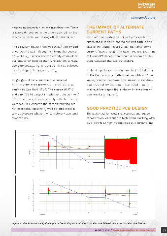
Single gate drivers, such as the isolated sistor, resolve this issue. The impact of carefully
EiceDRIVER™ 1EDI20N12AF, are the ideal com- dimensioned CM inductors that avoid compro-
panion to CoolGaN HEMT. The source (OUT+) mising driver capability is shown in the simula-
and sink (OUT-) outputs implement the turn-on/ tion results of figure 3.
off of the transistors separately with the correct
voltages. This ensures the gate thresholds are
not exceeded, keeping V well defined even at GOOD PRACTICE PCB DESIGN
G
low duty cycles where the RC network can tend The potential for stray inductances and capaci-
towards 0 V. tances to cause issues is high when working with
GaN HEMTs at high frequencies and current, and
Figure 2: In parallel CoolGaN™ operation, a high impedance in the Kelvin source path keeps severe oscillations in check.
Figure 3: Simulation showing the impact of switching 40 A without CM inductors (above) and with CM inductors (below).
20 MARCH 2021 | www.powerelectronicsnews.com MARCH 2021 | www.powerelectronicsnews.com 21