
Page 7 - PEN_Ebook_December_2021
P. 7
DESIGN Design
PARASITIC CURRENTS AT THE
SMPS INPUT
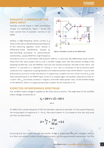
Parasitic currents result in radio-interference
voltage via impedances. Figure 1 shows the
main current flow of parasitic currents in an
SMPS.
Initially, a high-frequency active current (i )
DM
flows on the mains side with the pulse frequency
of the switching regulator, which results in
differential-mode interference. Caused by
Figure 1: Parasitic currents at the SMPS input
fast-switching processes of semiconductor
components, usually MOSFETs, high-frequency
oscillations occur in combination with parasitic effects. In principle, the differential-mode current
flows from the mains power line (L) over a rectifier bridge, then over the primary winding of the
isolating transformer, over the MOSFET, and over the neutral conductor (N) back to the mains. The
MOSFET is mounted on a heatsink for cooling. In turn, this is connected to the protective earth
conductor (PE). Capacitive coupling between the heatsink and the drain of the MOSFET occurs here
and produces common-mode interference. A capacitively coupled common-mode current (i ) now
CM
flows along PE back to the SMPS input, where it is coupled again via parasitic capacitance both on
L and N. The i now flows, as shown in Figure 1, over both mains power lines, via the rectifier bridge
CM
to the MOSFET, where it is again parasitically coupled via the heatsink to PE.
EXPECTED INTERFERENCE SPECTRUM
Line Filter: The Last The rectified mains voltage is applied at the drain-source section. The peak level of the rectified
mains voltage corresponds to:
Barrier in the
(Eq. 1)
Switch-Mode Power Supply An SMPS with a pulse frequency of 100 kHz has been used as an example. For this pulse frequency,
By Stefan Klein, application engineer at Würth Elektronik the timing signal corresponds to T = 10 µs. The pulse duration is 2 µs. Based on this, the duty cycle
can first be determined:
MOTIVATION FOR THE LINE FILTER
Switch-mode power supplies (SMPS) result in conducted interference because they generate
radio-interference voltage on the mains side. This can interfere with other equipment supplied (Eq. 2)
with mains power. Line filters help to suppress the generated radio-interference voltage. These can
easily be designed from passive components such as current-compensated line chokes and X/Y Assuming that the current through the rectifier bridge is trapezoidal, the EMC spectrum without
capacitors. This article concerns the design of a single-phase line filter. line filter and without further Fourier transformation can be approximately determined. The first
6 DECEMBER 2021 | www.powerelectronicsnews.com DECEMBER 2021 | www.powerelectronicsnews.com 7