
Page 53 - PEN eBook May 2023
P. 53
DESIGN DESIGN
SUMMARY
Deploying SiC in inverters will accelerate the adoption
of energy storage technologies and make them critical
elements of future grids. Integrating a BESS to an MV
grid through an isolated topology shows that using
3.3-kV single SIC MOSFETs enables higher system
efficiency, lower operating temperature and smallest
die size, compared with an equivalent silicon IGBT or
two 1,700-V SiC MOSFETs in series.
GeneSiC 3.3-kV SiC MOSFETs with monolithically
integrated monolithic MPS diodes achieve breakdown
voltages well above 3.3 kV and demonstrate smooth
switching performance while fully activating the
monolithic MPS diode. This significantly reduces power
losses in third-quadrant operation and enhances
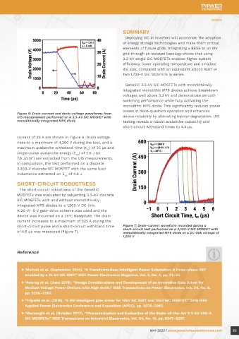
Figure 6: Drain-current and drain-voltage waveforms from
UIS measurement performed on a 3.3-kV SiC MOSFET with device reliability by alleviating bipolar degradation. UIS
Figure 4: Cross-sectional device schematic of 3.3-kV SiC MOSFET with monolithically integrated Schottky rectifier monolithically integrated MPS diode testing reveals a robust avalanche capability and
short-circuit withstand times to 4.5 µs.
3.3-kV/400-A silicon IGBT and a series connection of achieved by monolithically integrating a merged PiN current of 30 A are shown in Figure 6. Drain voltage
two 1.7-kV/325-A SiC MOSFETs from a third party in a Schottky (MPS) diode within the MOSFET. This enables rises to a maximum of 4,200 V during the test, and a
4.16-kV modular multi-level converter have revealed low conduction and switching-loss freewheeling diode maximum avalanche withstand time (t ) of 35 µs and
AV
significant benefits of the 3.3-kV SiC MOSFETs in operation without an externally connected Schottky single-pulse avalanche energy (E ) of 2.6 J (or
AS
MV applications. In general, the 3.3-kV SiC MOSFETs diode while reducing the parasitic inductance 7.6 J/cm ) are extracted from the UIS measurements.
2
reduced semiconductor losses and supported a smaller associated with an external diode connection. In comparison, the test performed on a discrete
installed semiconductor die area, improving the power Furthermore, this bypasses the built-in 3,300-V discrete SiC MOSFET with the same load
density of the system (including volume of heatsinks P-well/N-drift body diode of the D-MOSFET structure inductance extracted an E of 4.8 J.
AS
and fans). whose operation can induce faulting of the
basal-plane dislocations inevitably present within the SHORT-CIRCUIT ROBUSTNESS
3.3-KV SiC MOSFET WITH N-drift layer of the D-MOSFET. The short-circuit robustness of the GeneSiC
MONOLITHICALLY INTEGRATED MPS MOSFETs was evaluated by subjecting 3.3-kV discrete
DIODE Advantages include more efficient bidirectional SiC MOSFETs with and without monolithically
Further efficiency and reliability advantages can be performance, temperature-independent switching, integrated MPS diodes to a 1,200-V DC-link.
low switching and conduction losses, reduced cooling A 20-V/–5-V gate-drive scheme was used and the
requirements, superior long-term reliability, ease of device was mounted on a 25°C baseplate. The drain
paralleling and lower costs. current increases to a maximum of 525 A during the
short-circuit pulse and a short-circuit withstand time Figure 7: Drain-current waveform recorded during a
Navitas GeneSiC 3.3-kV discrete SiC MOSFETs and of 4.5 µs was measured (Figure 7). short-circuit test performed on a 3,300-V SiC MOSFET with
monolithically integrated MPS diode at a DC-link voltage of
SiC MOSFETs with monolithically integrated MPS 1,200 V
diodes typically have a breakdown-voltage range
of 3,600–3,900 V, well above the datasheet value.
When implementing a monolithic diode, there is a Reference
slightly higher drain-leakage current observed at
elevated voltages, due to the Schottky barrier lowering
under high electric fields. Figure 5 shows that in ▶ 1Mainali et al. (September 2014). “A Transformerless Intelligent Power Substation: A three-phase SST
tests, GeneSiC mono-SiC MOSFETs demonstrated enabled by a 15-kV SiC IGBT.” IEEE Power Electronics Magazine, Vol. 2, No. 3, pp. 31–43.
breakdown voltages in a range of 3.5 to 3.7 kV with
leakages ≈ 50 µA (or 0.3 mA/cm ) at the rated 3.3-kV ▶ 2Anurag et al. (June 2019). “Design Considerations and Development of an Innovative Gate Driver for
2
blocking voltage, for an R DS(on) of approximately 80 mΩ Medium Voltage Power Devices with High dv/dt.” IEEE Transactions on Power Electronics, Vol. 34, No. 6,
(measured). pp. 5256–5267.
▶ 3Tripathi et al. (2016). “A MV intelligent gate driver for 15kV SiC IGBT and 10kV SiC MOSFET.” 2016 IEEE
Unclamped inductive switching (UIS) measurements Applied Power Electronics Conference and Exposition (APEC), pp. 2076–2082.
were used to investigate avalanche robustness of the
Figure 5: Third-quadrant breakdown characteristic measured 3,300-V SiC MOSFETs with integrated MPS diodes. ▶ 4Marzoughi et al. (October 2017). “Characterization and Evaluation of the State-of-the-Art 3.3-kV 400-A
on 3.3-kV SiC MOSFETs with monolithically integrated MPS SiC MOSFETs.” IEEE Transactions on Industrial Electronics, Vol. 64, No. 10, pp. 8247–8257.
diodes The drain-current/-voltage waveforms at a peak drain
52 MAY 2023 | www.powerelectronicsnews.com MAY 2023 | www.powerelectronicsnews.com 53