
Page 57 - EE Times Europe November 2021 final
P. 57
EE|Times EUROPE 57
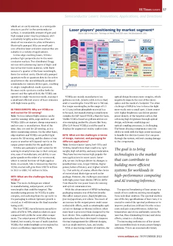
Semiconductor Lasers: Innovations, Applications, and Directions
which act as cavity mirrors, in a waveguide
structure parallel to the semiconductor
surface. A considerable amount of gain and
high output power may be produced, with
a relatively lengthy active area of hun-
dreds of micrometers to a few millimeters.
Electrically pumped EELs are small and
cost-effective laser-emission sources that are
suitable in a variety of applications.
Unlike edge-emitting lasers, VCSELs
produce light perpendicular to the semi-
conductor surface. Two distributed Bragg
mirrors with alternating layers of high- and
low-refractive–index material, with thick-
nesses of a quarter of the laser wavelength,
form the vertical cavity. Electrically pumped
quantum wells or quantum dots in the active
area between the monolithically produced
semiconductor mirrors deliver gain, resulting
in single-longitudinal–mode operation.
Because oxide apertures confine both the
current and the optical field, the VCSEL can
operate in single-transverse mode, making it VCSELs are mainly manufactured on optical design becomes more complex, which
a small and efficient source of laser emission gallium arsenide, [which yields devices that] negatively impacts the cost of the micro-
with high beam quality. emit at wavelengths from 850 nm to 940 nm. optics and the module’s footprint. The other
For longer wavelengths, in the range of 1.3 challenge of HPLD is how to focus the light
EE TIMES EUROPE: Why are VCSELs so or 1.5 µm, indium phosphide material has more easily onto a small spot. A laser source
well-suited for 3D sensing? to be used, but manufacturing is much more with higher brightness can deliver greater
Yole: Various infrared light sources can be complex for InP-based VSCELs than for GaAs. power density at the targeted surface, but
used for sensing: LEDs, edge emitters, and Visible VCSELs based on gallium nitride are achieving high brightness through optical
VCSELs. LEDs are mature, cheap components also emerging, pushed by players like Sony. design, with beam-combining and
and are easy to manufacture. Most of the [The GaN-based VCSELs] could be used in optical-coupling processes, is challenging.
time, they are used for 2D sensing, as in a displays for augmented-reality applications. The beam-shaping components need the
driver-monitoring system. On the other hand, ability to work with the high power necessary
edge emitters and VCSELs are perfect light EETE: What are the challenges in terms to handle the electrical power that can pass
sources for 3D sensing, and the choice of one of design, material, and packaging for through the system, without causing damage
source or another will depend mainly on the different applications? to the components.
output power needed for the application. Yole: Semiconductor lasers, both EELs and
VCSELs are particularly well-suited for 3D VCSELs, benefit from their small size, light The goal is to bring
sensing in smartphones due to their compact weight, high reliability, and easy modulation.
size, ease of manufacture, and ability to use They have become increasingly popular for technologies to the market
pulse speeds on the order of a nanosecond, new applications in recent years. Gener-
which is needed for time-of-flight applica- ally, we see challenges driven by changes to that can contribute to
tions. As a result, Yole is forecasting that the [enable] lower cost, longer lifetime, higher building more efficient
VCSEL market will grow from US$794 million power, better efficiency, and [higher] reliabil-
in 2021 to US$1,742 million in 2026. ity. That activity, of course, affects the choice systems for workloads in
of material and diode type as well as the high-performance computing
EETE: What are the challenges facing package. However, the challenges associated
VCSELs? with high-power laser diodes [HPLDs] differ and AI training/inference.
Yole: The main challenges are related from those for low-power lasers for sensing
to manufacturing, output power, and the and optical communication.
wavelengths that could be targeted. The With the advancement of HPLD technology, The spectral broadening of laser arrays is a
manufacturing process for VCSELs is quite packaging remains one of the bottlenecks result of non-uniform emitting wavelengths
complex, and each step from the epi wafer to that affect output power, [high] brightness, from individual emitters. The spectral width is
the packaging is critical. Epitaxial growth is [narrow] spectrum, and others. Too much of one of the key specifications of laser bars; it is
crucial, as it will determine the final manufac- an increase in the output power could cause crucial to control the spectral performance to
turing yield. undesirable effects, such as catastrophic opti- improve production yield and thereby reduce
The best VCSEL manufacturers can achieve cal mirror damage or thermal rollover, when costs and gain competitiveness. Achieving
yields of 65% to 70%, which is relatively poor more heat is generated than dissipated by the temperature and stress uniformity across the
compared with yields for some other compo- laser device. New, sophisticated packaging laser bar, thus eliminating thermal and stress
nents. The output power of VCSELs has been approaches have been developed to improve effects, remains a challenge.
limited, but recently, the use of multi-junction thermal management for different designs, The increasing performance of low-power
VCSELs that embed multiple active regions has such as single emitters, bars, and stacks. laser assemblies leads to many power-hungry
shown an efficiency improvement of 30%. With an increasing number of emitters, the solutions. This is an unsustainable trend,
www.eetimes.eu | NOVEMBER 2021