
Page 39 - EE|Times Europe Magazine - December 2020
P. 39
EE|Times EUROPE 39
MARKET & TECHNOLOGY TRENDS
Aledia’s Future Is on MicroLED Display
By Anne-Françoise Pelé
Any intention to build a plant during these unprecedented times of the Covid-19
pandemic deserves attention. EE Times Europe takes you to the Grenoble valley,
France’s epicenter of microelectronics production, for a discussion with Giorgio Anania,
co-founder and CEO of Aledia, a developer and manufacturer of 3D microLEDs for
display applications.
re microLEDs the next big thing for display technology? Will display market, chips must be small.
they displace LEDs? Lately, microLEDs have garnered a lot The efficiency of each nanowire does
of attention in the display industry, and the global market is not change even with smaller chip
Aexpected to grow from just 1,000 units in 2020 to 15.5 million sizes, which isn’t the case for tradi-
units in 2026, as a sharp drop in manufacturing costs over the forecast tional LEDs.” Aledia started to focus
period makes this emerging technology suitable for the mass market, on displays in 2016 and claims it is
according to market research firm IHS Markit. the only company in the world that
With a €120 million investment plan, Aledia aims to cement its has reached the commercial stage
position in the microLED display market by bringing advanced micro- with nanowires.
electronics manufacturing technology to the world of displays. The 3D structure with nanowires
Spun out of CEA-Leti in 2012, Aledia develops and manufactures may offer resolution, brightness,
microLED chips based on a 3D architecture using gallium- and reliability advantages, but it
nitride-on-silicon nanowires. Its LEDs are built on 8-inch (200-mm) is complex to optimize. There are
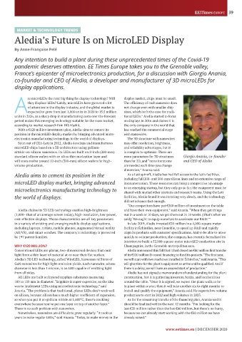
standard silicon wafers with an ultra-thin nucleation layer and more parameters for 3D structures Giorgio Anania, co-founder
will soon evolve toward 12-inch (300-mm) silicon wafers for high- than for 2D, and “more iterations and CEO of Aledia
volume production. are needed each time you change
dimension,” Anania said.
Aledia aims to cement its position in the As a Leti spinoff, Aledia has had full access to the lab’s facilities,
microLED display market, bringing advanced including full 200- and 300-mm silicon lines and an extensive range of
instrumentation. Those resources can bring a competitive advantage
microelectronics manufacturing technology to to an emerging startup, but they only go so far; the equipment must be
shared with myriad other startups and research teams. Using the Leti
the world of displays. facilities, Aledia found it was iterating very slowly, and the technology
did not advance fast enough.
“Our competitors have put €200 million of investment on the table
Aledia claims its 3D LED technology enables high-brightness and have their own equipment,” said Anania. “When they get things
(1,000× that of an average screen today), high-resolution, low-power, out in a week or 10 days, we get them out in 10 weeks. [That’s when we
cost-effective displays. Those characteristics are all key parameters said,] ‘We ought to equip ourselves to accelerate our R&D.’ ”
in a variety of existing and emerging mobile display applications, In late 2019, Aledia invested €20 million in a 4,000-square-meter
including laptops, tablets, mobile phones, augmented/virtual reality facility in Échirolles, near Grenoble, to speed up R&D and rapidly
(AR/VR), and smart watches. The company’s technology is protected align its products with customer specifications. And to be able to move
by 197 patent families. quickly to volume production, the company has recently formalized its
intention to build a 52,000-square-meter microLED production site in
WHY €120 MILLION? Champagnier, in the Grenoble metropolitan area.
Conventional LEDs are planar, two-dimensional devices that emit Aledia announced this fall that it had closed an €80 million first tranche
light from a thin layer of material at or near their flat surface. of its €120 million D-round financing to fund its projects. “The first year,
Aledia’s 3D LED technology, called WireLED, harnesses millions of we will start with two machines installed in Échirolles,” said Anania. “This
GaN nanowires for high light-emission yields. Each nanowire, whose will give time for the plant’s equipment to arrive and be qualified. And if
diameter is less than 1 micron, is an LED capable of emitting light there is a delay, we will have an assured start of production.”
from all sides. Aledia has not signed a memorandum of understanding for the plant
All LEDs are built on layered sapphire substrates measuring construction, but it is gathering investors, banks, and local entities
100 to 150 mm in diameter. “Sapphire is super-expensive, so the idea around the table. “Once it is signed, we expect the plant walls to be
was to implement LEDs using microelectronic technology,” said in place within a year; then it will take another six to eight months to
Anania. “The problem is that traditional, planar LEDs don’t work well install and qualify the equipment,” Anania said. He expects low-volume
on silicon, because silicon has a much higher coefficient of expansion, production to start in 2022 and high volumes in 2023.
so when you put it on gallium nitride at 1,000°C, there’s crackling As for the remaining tranche of the financing plan, Anania said it
everywhere because you’ve put one layer on top of another layer.” should be finalized within the next 12 months. “I’m looking for the
There is no such problem with nanowires. last €20 million rather than the last €40 million, but there’s no hurry,
Nonetheless, nanowires are difficult to grow regularly. “It took us because we can already start working with the €80 million we have
years to make regular LEDs,” said Anania. “Today, to make money in the already raised.”
www.eetimes.eu | DECEMBER 2020