
Page 29 - PEN eBook October 2022
P. 29
SEMICONDUCTORS Semiconductors
In addition to the consideration on the breakdown voltage, enhancement-mode GaN transistors
feature the two-dimensional electron gas (2DEG), which is formed between the GaN layer and a
thin layer of AlGaN. The 2DEG’s high electron mobility lowers the device’s on-resistance, keeping
its dimensions small.
The shorter width of the drift region, due to the higher critical field and the high electron mobility
of the 2DEG, allows the use of lateral conduction devices. One of the advantages of lateral devices
with respect to vertical conduction devices is that more devices can be integrated on the same
substrate, such as half-bridge circuits.
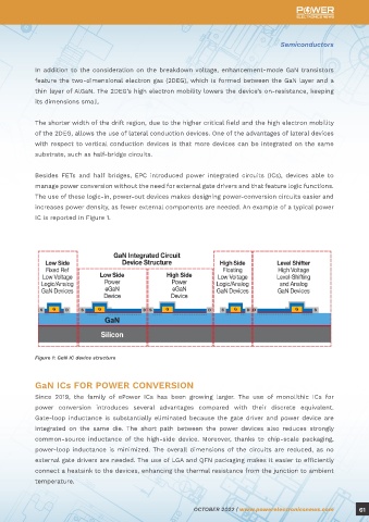
Besides FETs and half bridges, EPC introduced power integrated circuits (ICs), devices able to
manage power conversion without the need for external gate drivers and that feature logic functions.
GaN ePower Stage ICs The use of these logic-in, power-out devices makes designing power-conversion circuits easier and
increases power density, as fewer external components are needed. An example of a typical power
Bring Logic-In, IC is reported in Figure 1.
Power-Out Simplicity
to Motor Drive Applications
By Federico Unnia, application engineer at EPC
Gallium nitride devices are leading the innovation in power conversion. The benefits of GaN-based
inverters are becoming increasingly evident in motor drive applications.
The advantages of GaN technology are presented in Reference 1, and a glimpse of some physical Figure 1: GaN IC device structure
properties of GaN and silicon are reported in Table 1.
The critical field is one of the GaN ICs FOR POWER CONVERSION
properties mentioned above, and it Since 2019, the family of ePower ICs has been growing larger. The use of monolithic ICs for
determines the breakdown voltage power conversion introduces several advantages compared with their discrete equivalent.
of a device; these two properties Gate-loop inductance is substantially eliminated because the gate driver and power device are
are related by the width of the integrated on the same die. The short path between the power devices also reduces strongly
drift region. For a given breakdown common-source inductance of the high-side device. Moreover, thanks to chip-scale packaging,
voltage, the higher the electric power-loop inductance is minimized. The overall dimensions of the circuits are reduced, as no
Table 1: Physical properties of silicon vs. GaN
field, the shorter the width of the external gate drivers are needed. The use of LGA and QFN packaging makes it easier to efficiently
drift region. The critical field is one connect a heatsink to the devices, enhancing the thermal resistance from the junction to ambient
order of magnitude higher in GaN technology, which allows for much smaller devices. temperature.
60 OCTOBER 2022 | www.powerelectronicsnews.com OCTOBER 2022 | www.powerelectronicsnews.com 61