Page 32 - PEN Ebook March 2021
P. 32

Power Supply                                                                                                                                                                                                  Power Supply


                                                      (a)      are visible. On the right-hand side, the output                                                                                         There are three reasons for
                                                               FET is visible. This device will take a logic signal                                                                                    the higher performance of the
                                                               and send out a very high current and a very, very                                                                                       monolithic power stage. First,
                                                               short pulse to fire a laser in a time-of-flight lidar                                                                                   the power loop inductance is
                                                               application. This is an excellent example of how                                                                                        significantly reduced by making
                                                               integrating the driver plus the GaN field effect                                                                                        a monolithic half bridge. Sec-
                                                               transistor on one chip generates an extremely                                                                                           ondly, the gate loop inductance
                                                               powerful and very fast IC that can be driven off a                                                                                      in eliminated by putting the
                                                                                                                                 Figure 5: Cross section diagram of an eGaN integrated power stage.
                                                               regular logic gate.                                                                                                                     drivers on the same chip locat-
                                                                                                                                 and at 2.5 MHz in a 48 V  – 12 V OUT  buck con-      ed extremely close to the FETs. Lastly, by putting
                                                                                                                                                         IN
                                                      (b)
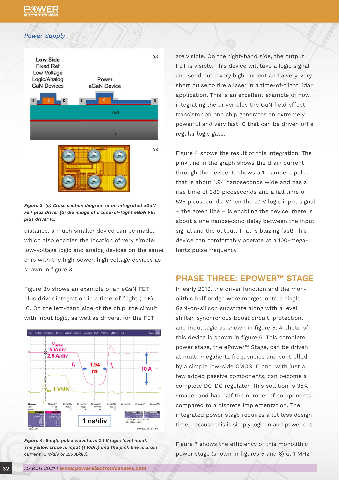
                                                               Figure 4 shows the result of this integration. The                verter. The green line shows the efficiency of the   all these components together, a thermal tub
                                                               pink line in the graph shows the drain current                    monolithic power stage, and the blue line rep-       is created that balances the temperature of all
                                                               through the device. It shows a 10-ampere pulse                    resents that of a discrete implementation using      the devices, so there is a net, on average, lower
                                                               that is about 1.94 nanoseconds wide and has a                     FETs with the same characteristics as those on       temperature. The dotted lines on the graph are
                                                               rise time of 380 picoseconds and a fall time of                   the monolithic IC and utilizing a very efficient     the same devices at 2.5 MHz. The black X repre-
                                                               525 picoseconds. When the 2.1 V logic input signal                                                                     sents the best performance that the aging power
          Figure 3: (a) Cross section diagram of an integrated eGaN
          FET plus driver (b) die image of a time-of-flight eGaN FET   – the green line – is enabling the device, there is                                                            MOSFETs can achieve in this application.
          plus driver IC.                                      about a one nanosecond delay between the input

          distance, a much smaller device can be made,         signal and the output. That is blazing fast! This
          which also enables the location of very simple,      device can comfortably operate at a 100-mega-
          low-voltage logic and analog devices on the same     hertz pulse frequency.
          chip with the high power, high voltage devices as
          shown in figure 3.
                                                               PHASE THREE: EPOWER™ STAGE
          Figure 3b shows an example of an eGaN FET            In early 2019, the driver function and the mon-
          plus driver integration in a time-of-flight (ToF)    olithic half bridge were merged onto a single                     Figure 6: Die image of the EPC2152, ePower™ Stage.

          IC. On the left-hand side of the chip, the circuit   GaN-on-silicon substrate along with a level                       layout with a discrete driver IC placed very close
          with input logic, as well as drivers, for the FET    shifter, synchronous boost circuit, protection,                   to the FETs. The solid lines shown on the graph
                                                                                                                                                                                      Figure 7: Performance comparison of GaN discrete (blue
                                                               and input logic as shown in figure 5. A photo of                  are at 1 MHz and the performance of the mono-
                                                                                                                                                                                      line) and GaN monolithic half bridge (green line) in a 48 V
                                                               this device is shown in figure 6. This complete                   lithic IC is substantially better than the discrete   input, 12 V output buck converter operating at 1 MHz (solid
                                                               power stage, the ePower™ Stage, can be driven                     implementation.                                      line) and 2.5 MHz (dotted line). Best-in-class MOSFET
                                                                                                                                                                                      performance at 1MHz shown with the black X.
                                                               at multi-megahertz frequencies and controlled
                                                               by a simple low-side CMOS IC and, with just a

                                                               few added passive components, can become a
                                                               complete DC-DC regulator. This solution is 35%
                                                               smaller and has half the number of components
                                                               compared to a discrete implementation. The
                                                               integrated power stage requires a lot less design
                                                               time, because this is simply logic in and power out.


          Figure 4: Single pulse waveform 2.1 V logic level input.   Figure 7 shows the efficiency of this monolithic
          The yellow trace is input (1 V/div) and the pink line is drain
          current (5 V/div or 2.5 A/div).                      power stage (shown in figures 5 and 6) at 1 MHz

  32      MARCH 2021 | www.powerelectronicsnews.com                                                                                                                                         MARCH 2021 | www.powerelectronicsnews.com       33
   27   28   29   30   31   32   33   34   35   36   37