
Page 49 - Power Electronics News - December 2020
P. 49
Test & Measurements Test & Measurements
and internal chip power distribution, but every in- the design. Notice the large coinciding spur at the red and every active component can
terconnect, trace, via, connector, capacitor, pack- marker in Figure 4. The TIE histogram to the right of alter the voltages of power rails
age, pins, and ball-grids. the TIE spectrum has the signature sinusoidal jitter and ground planes.
distribution (horseshoe), PJ at one frequency.
The eye diagram can tell us a
THE IMPACT OF RIPPLE ON Power supplies can introduce random noise that lot about signal integrity, but it
RANDOM AND PERIODIC JITTER contributes to RJ. The power rail random noise rarely helps us identify specific
Power rail noise, often called ripple, is typically a shows up as the noise floor of the Spectrum View problems. Analysis of the TIE
few millivolts. Accurate measurements of mV noise plot in the upper left in Figure 4. RJ is calculated distribution breaks jitter into
on a power rail at GHz frequencies requires high from the noise floor of the TIE spectrum. In this components that provide clues
bandwidth probes with high DC impedance that example, the random noise due to power ripple is of where problems lie. High RJ
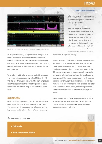
act as 50 Ω transmission lines at high-frequencies. very low, and RJ is tiny, about 0.84 ps. Figure 5: Power rail ripple spectrum and TIE/ jitter spectrum. usually means a noisy clock,
Power rail probes are designed explicitly for this but it can also indicate random
purpose. or Nyquist frequency and perhaps as many as two noise from the power supply.
PJ & GROUND BOUNCE higher harmonics, plus the subharmonics from
Switch-mode power supplies regulate the voltage During logic transitions, transmitters and receivers consecutive identical bits. Simultaneous switching PJ can indicate a faulty clock, power supply switch-
between the power rail and the return path (a.k.a., source or sink current from the PDN. When multi- can occur at any of these frequencies. Thus, SSN is ing noise, or ground bounce/SSN. Comparing the
“ground”) by continuously switching between low ple signals switch between levels simultaneously, periodic noise with many low amplitude spurs that power rail ripple spectrum to the TIE spectrum
dissipation on and off states. Unfortunately, the they can deposit or remove substantial charge from can cause PJ. can isolate the problem in two steps. Spurs in the
pulses that drive the switching elements can in- the power rail and/or ground plane. The short-term TIE spectrum without any corresponding spurs in
duce “switching noise” and cause PJ. introduction of charge density alters the voltage To confirm that the PJ is caused by SSN, compare the power rail spectrum indicate the clock; one or
of what should be a common ground across the the power rail spectrum, top left of Figure 5, with two spurs at the same frequencies in both spectra
Switching occurs at fixed frequencies that should conductor. The resulting voltage variation is called the TIE spectrum, just below it. The high amplitude indicate power supply switching noise; and a large
be recorded on the DC-to-DC converter data sheet. ground bounce or, equivalently, simultaneous spur that appears at the same frequency in both number of spurs common to both spectra indicates
If the ripple spectrum, top left of Figure 4, and the switching noise (SSN). spectrums indicates a large PJ contribution from SSN. In each of these cases, combining jitter and
TIE spectrum, just below it, both have spurs at the SSN. power analysis isolates otherwise difficult prob-
switching frequencies or harmonics of switching fre- Before continuing, we should clarify a couple of lems.
quencies, then we know the source and can address things. First, by “ground” we’re referring to the de-
sired common reference volt- SUMMARY Signal integrity and power integrity are often con-
age of the return path which is Signal integrity and power integrity are a feedback sidered separate disciplines, but we’ve seen that
usually defined to be 0 V. Sec- loop. Every element of the network, every trace, finding problems associated with high jitter re-
ond, “simultaneous” means that via, connector, pin, package, etc, affects the PDN quires understanding both.
the components source or sink impedance and the impedance of every channel,
charge during the time interval
when their rise/fall times over-
lap. For More Information
SSN looks random in the time
domain but not in the frequen- ▶ Tektronix
cy domain. Data signals are
composed of many frequency ▶ How to measure Ripple
Figure 4: : Power rail ripple in Spectrum View top left, and TIE spectrum just below
it, along with the signal and power rail waveforms and the TIE histogram. components—the fundamental
48 DECEMBER 2020 | www.powerelectronicsnews.com DECEMBER 2020 | www.powerelectronicsnews.com 49