
Page 30 - EE Times Europe September 2021
P. 30
30 EE|Times EUROPE EE|Times EUROPE 30
30 EE|Times EUROPE
Enhancing Efficiency by Reducing Converter Stages and R in Power Management ICs
Embedding Security at the Edge ON
When this switching noise is introduced
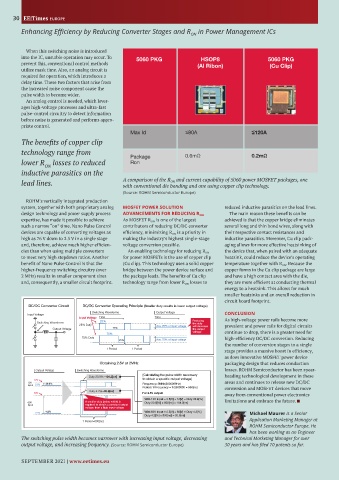
into the IC, unstable operation may occur. To 5060 PKG HSOP8 5060 PKG
prevent this, conventional control methods (Al Ribon) (Cu Clip)
utilize mask time. Also, an analog circuit is
required for operation, which introduces a
delay time. These two factors that arise from
the increased noise component cause the
pulse width to become wider.
An analog control is needed, which lever-
ages high-voltage processes and ultra-fast
pulse-control circuitry to detect information
before noise is generated and performs appro-
priate control.
Max Id ≤ 80A ≤ 120A
The benefits of copper clip
technology range from Package 0.6mΩ 0.2mΩ
lower R losses to reduced Ron
ON
inductive parasitics on the
lead lines. A comparison of the R ON and current capability of 5060 power MOSFET packages, one
with conventional die bonding and one using copper clip technology.
(Source: ROHM Semiconductor Europe)
ROHM’s vertically integrated production
system, together with both proprietary analog MOSFET POWER SOLUTION reduced inductive parasitics on the lead lines.
design technology and power supply process ADVANCEMENTS FOR REDUCING R ON The main reason these benefits can be
expertise, has made it possible to achieve As MOSFET R ON is one of the largest achieved is that the copper bridge eliminates
such a narrow “on” time. Nano Pulse Control contribu tors of reducing DC/DC converter several long and thin bond wires, along with
devices are capable of converting voltages as efficiency, minimizing R ON is a priority in their respective contact resistances and
high as 76 V down to 2.5 V in a single stage making the industry’s highest single-stage inductive parasitics. Moreover, Cu clip pack-
and, therefore, achieve much higher efficien- voltage conversion possible. aging allows for more effective heatsinking of
cies than when using multiple converters An enabling technology for reducing R ON the device that, when paired with an adequate
to meet very high stepdown ratios. Another for power MOSFETs is the use of copper clip heatsink, could reduce the device’s operating
benefit of Nano Pulse Control is that the (Cu clip). This technology uses a solid copper temperature together with R ON . Because the
higher-frequency switching circuitry (over bridge between the power device surface and copper forms in the Cu clip package are large
2 MHz) results in smaller component sizes the package leads. The benefits of Cu clip and have a high contact area with the die,
and, consequently, a smaller circuit footprint. technology range from lower R ON losses to they are more efficient at conducting thermal
energy to a heatsink. This allows for much
smaller heatsinks and an overall reduction in
circuit board footprint.
DC/DC Converter Circuit DC/DC Converter Operating Principle (Smaller duty results in lower output voltage)
Switching Waveforms Output Voltage
Input Voltage CONCLUSION
Input Voltage Time Time As high-voltage power rails become more
25% Reducing
Switching Waveforms the duty
25% Duty Ave. 25% of input voltage will decrease prevalent and power rails for digital circuits
Output Voltage 75% the output
voltage continue to drop, there is a greater need for
75%
75% Duty high-efficiency DC/DC conversion. Reducing
25% Ave. 75% of input voltage
the number of conversion stages to a single
1 Period 1 Period
stage provides a massive boost in efficiency,
as does innovative MOSFET power device
Obtaining 2.5V at 2MHz packaging design that reduces conduction
Output Voltage Switching Waveforms losses. ROHM Semiconductor has been spear-
[Calculating the pulse width necessary
Duty 20.8%=104.2[ns] heading technological development in these
12V to obtain a specific output voltage]
12V 20.8% Frequency: 2MHz(2000000Hz) areas and continues to release new DC/DC
Input 2.5V
Period: 1/Frequency = 1/2000000 = 500[ns] conversion and MOSFET devices that move
Duty 4.2%=20.8[ns]
60V For 2.5V output: away from conventional power electronics
With 12V Input = 2.5[V] + 12[V] = Duty 20.8[%]
60V A smaller duty (pulse width) is Duty 20.8[%] x 500[ns] = 104.2[ns] limitations and embrace the future. ■
Input required to obtain a constant output
voltage from a high input voltage
4.2% With 60V Input = 2.5[V] + 60[V] = Duty 4.2[%]
2.5V Michael Maurer is a Senior
Duty 4.2[%] x 500[ns] = 20.8[ns]
Application Marketing Manager at
1 Period=500[ns]
ROHM Semiconductor Europe. He
has been working as an Engineer
The switching pulse width becomes narrower with increasing input voltage, decreasing and Technical Marketing Manager for over
output voltage, and increasing frequency. (Source: ROHM Semiconductor Europe) 30 years and has filed 10 patents so far.
w
w
SEPTEMBER 2021 | www.eetimes.eu www.eetimes.eu | SEPTEMBER 2021
w
|
.eetimes.eu
1
2
2
SEPTEMBER
0