
Page 32 - EE Times Europe November 2021 final
P. 32
32 EE|Times EUROPE
SPECIAL REPORT: ARTIFICIAL INTELLIGENCE
Memory Bottlenecks: Overcoming a Common
AI Problem
By Sally Ward-Foxton
keptics of artificial intelligence have
criticized the memory bottleneck
that exists in the current technology,
Sarguing that the inability to accelerate
the data movement between processor and
memory is holding back useful real-world
applications.
AI accelerators used to train AI models
in data centers require the highest memory
bandwidth available. While storing an entire
model in a processor would eliminate off-chip
memory from the equation, it isn’t a feasible
solution, as the largest models measure in the
billions or trillions of parameters.
Where yesterday’s systems were
memory-constrained, today’s data center
architectures use a variety of techniques to
overcome memory bottlenecks.
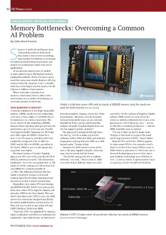
Nvidia’s A100 data center GPU with six stacks of HBM2E memory (only five stacks are
HIGH-BANDWIDTH MEMORY used, for yield reasons) (Source: Nvidia)
A popular solution is to use high-bandwidth
memory (HBM), which involves connecting principal engineer, during a recent Hot Chips controller. On the version of Sapphire Rapids
a 3D stack of four, eight, or 12 DRAM dies to presentation. “However, with the exponen- without HBM, there’s an area of the die
the processor via a silicon interposer. The tially growing model sizes, we see constant where we added accelerators for crypto, com-
latest version of the technology, HBM2E, demand for both capacity and bandwidth pression, etc. All of those go away — except
features faster signaling rates per pin than its without tradeoffs. Sapphire Rapids does just for the data-streaming accelerator — and the
predecessor, up to 3.6 Gb/s per pin, thereby that by supporting both, natively.” HBM controller goes in instead.
boosting bandwidth. Samsung and SK Hynix The approach is enhanced through mem- “On top of that, we had to make some
each offer eight-die HBM2E stacks for a ory tiering, “which includes support for changes to the mesh to support the band-
total of 16-GB capacity, providing 460-GB/s software-visible HBM plus DDR, and software width requirements of HBM,” Nassif added.
bandwidth (compared with 2.4 GB/s for transparent caching that uses HBM as a DDR- Beyond CPUs and GPUs, HBM is popular
DDR5 and 64 GB/s for GDDR6, according to backed cache,” Biswas added. for data center FPGAs. For example, Intel’s
SK Hynix). HBM3 is set to push speeds and However, the HBM versions come at the Stratix and the Xilinx Versal FPGAs come in
capacities even higher. cost of die area, Sapphire Rapids’ chief engi- HBM versions, and some AI ASICs also use it.
The latest version of Nvidia’s flagship neer, Nevine Nassif, told EE Times. Tencent-backed data center AI ASIC devel-
data center GPU, the A100, provides 80 GB of “The [HBM-compatible] die is slightly oper Enflame Technology uses HBM for its
HBM2E performance with 2 TB/s of memory different,” she said. “There’s also an HBM DTU 1.0 device, which is optimized for cloud
bandwidth. The A100 incorporates five 16-GB controller that is different than the DDR5 AI training. The 80-TFLOPS (FP16/BF16)
stacks of DRAM, joining a 40-GB version that
uses HBM2 for a total bandwidth of
1.6 TB/s. The difference between the two
yields a threefold increase in AI model
training speed for the deep-learning recom-
mendation model, a known memory hog.
Meanwhile, data center CPUs are leverag-
ing HBM bandwidth. Intel’s next-generation
Xeon data center CPUs, Sapphire Rapids, will
introduce HBM to the Xeon family. They are
Intel’s first data center CPUs to use new AMX
instruction extensions designed specifically
for matrix multiplication workloads like AI.
They will also be able to use either off-chip
DDR5 DRAM or DRAM plus HBM.
“Typically, CPUs are optimized for capacity,
while accelerators and GPUs are optimized for Enflame’s DTU 1.0 data center AI accelerator chip has two stacks of HBM2 memory.
bandwidth,” said Arijit Biswas, an Intel senior (Source: Enflame Technology)
NOVEMBER 2021 | www.eetimes.eu