Page 38 - EETimes Europe June 2021
P. 38
38 EE|Times EUROPE


           OPINION | EV & AV


           Driving for Perfection: SiC


           Semiconductors in EVs


           By Anup Bhalla, UnitedSiC


           EVS ARE PACKED WITH ELECTRONICS requiring power. For high efficiency, switched-
           mode techniques are used to generate voltage rails, relying on semiconductors operating at high   The ideal switch
           frequency. The ideal switch for the application has near-zero resistance when on, no leakage
           when off, and a high breakdown voltage. When it transitions between states, there should be   input and 390-VDC output using 18- or 60-mΩ
           little transient power dissipation, and any residual losses should result in minimal switch tem-  GEN 4 SiC FETs in TO-247-4L packages, switch-
           perature rise. The search continues for the perfect switch.             ing at 60 kHz. System efficiency plots show a
             IGBTs are favored at very high power for their low conduction losses, while MOSFETs domi-  peak value of 99.37% achieved at 230 VAC with
           nate at low to medium power, where their fast switching minimizes associated component size   one 18-mΩ SiC FET used for the high-
           and cost. MOSFETs traditionally use silicon technology, but now, silicon carbide can be employed   frequency, high-and low-side switch positions.
           to leverage its low dynamic and conduction losses and its high-temperature operation. An even   At full 3.6-kW output, the SiC FETs require
           better approach is the SiC FET — a SiC JFET co-packaged with a low-voltage Si MOSFET in a   minimal heatsinking. ■
           cascode arrangement. The Si MOSFET provides for an easy, non-critical gate drive, while turning
           the normally on JFET into a normally off cascode.                       Anup Bhalla is vice president of engineering
             The higher critical breakdown voltage of SiC in a MOSFET or JFET allows for a much thinner   at UnitedSiC. This presentation summary
           drift layer than in a silicon IGBT. Si IGBTs achieve low resistance by injecting a high number of   appears as part of the proceedings of EE Times’
           carriers into the thicker drift layer, leading to a 100× stored charge, which has to be swept in and   Roadmap to Next-Gen EV & AV virtual confer-
           out of the drift layer in each switching cycle. This results in relatively high switching loss and   ence, now available for download on Power
           significant gate-drive power requirements. SiC MOSFETs and JFETs are unipolar devices in which   Electronics News.
           charge movement is just in and out of device capacitances, minimizing
           dynamic losses.
             Electron mobility in the channel is much better with a SiC FET than
           with a SiC MOSFET, allowing a smaller die for the same resistance, with
           lower capacitance and faster switching or lower on-resistance for the
           same die area. This enables a higher die count per wafer for a given per-
           formance and consequent cost savings or a lower conduction loss for a
           given die area. The win-win of more dies per wafer with faster switching
           is tempered by the need to remove heat from a smaller area. SiC has
           3× better thermal conductivity than Si and can operate at higher average
           and peak temperatures, but to enhance reliability, GEN 4 SiC FETs use
           wafer thinning to reduce the electrical and thermal resistance and a
           silver sinter die-attach for 6× better thermal conductivity than solder.
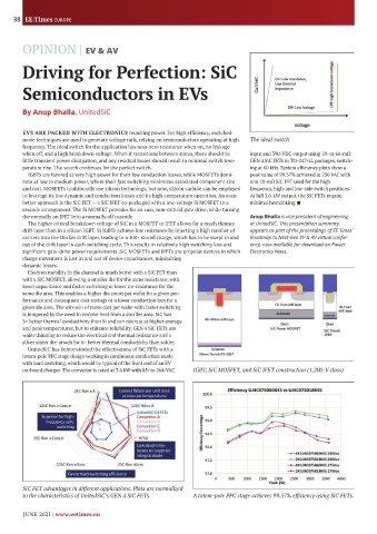
             UnitedSiC has demonstrated the effectiveness of SiC FETs with a
           totem-pole PFC stage design working in continuous conduction mode
           with hard switching, which would be typical of the front end of an EV
           on-board charger. The converter is rated at 3.6 kW with 85- to 264-VAC   IGBT, SiC MOSFET, and SiC JFET construction (1,200-V class)


           SiC FET advantages in different applications. Plots are normalized
           to the characteristics of UnitedSiC’s GEN 4 SiC FETs.  A totem-pole PFC stage achieves 99.37% efficiency using SiC FETs.

           JUNE 2021 | www.eetimes.eu

