
Page 39 - EETEurope FlipBook February
P. 39
EE|Times EUROPE — Power Electronics 39
GaN Evaluation Board for AC/DC Power Conversion
to develop control firmware, as is required for
solutions based on digital signal controllers.
The GaN-based platform provides the
reliability of wide-bandgap semiconductor
physics and ensures ease of design drive-
ability and high-volume reproducibility.
Transphorm said its approach offers designers
a more efficient power supply system than
is achievable with standard continuous con-
duction mode (CCM) boost PFC designs using
superjunction MOSFETs.
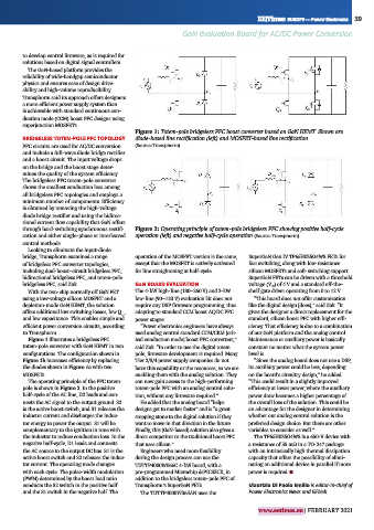
Figure 1: Totem-pole bridgeless PFC boost converter based on GaN HEMT. Shown are
BRIDGELESS TOTEM-POLE PFC TOPOLOGY diode-based line rectification (left) and MOSFET-based line rectification.
PFC circuits are used for AC/DC conversion (Source: Transphorm)
and include a full-wave diode bridge rectifier
and a boost circuit. The input voltage drops
on the bridge and the boost stage deter-
mines the quality of the system efficiency.
The bridgeless PFC totem-pole converter
shows the smallest conduction loss among
all bridgeless PFC topologies and employs a
minimum number of components. Efficiency
is obtained by removing the high-voltage
diode bridge rectifier and using the bidirec-
tional current flow capability that GaN offers
through hard-switching synchronous rectifi- Figure 2: Operating principle of totem-pole bridgeless PFC showing positive half-cycle
cation and either single-phase or interleaved operation (left) and negative half-cycle operation (Source: Transphorm)
control methods.
Looking to eliminate the input-diode
bridge, Transphorm examined a range operation of the MOSFET version is the same, SuperGaN Gen IV TP65H035G4WS FETs for
of bridgeless PFC converter topologies, except that the MOSFET is actively activated fast switching, along with low-resistance
including dual-boost–circuit bridgeless PFC, for line straightening at half-cycle. silicon MOSFETs and soft-switching support.
bidirectional bridgeless PFC, and totem-pole SuperGaN FETs can be driven with a threshold
POWER ELECTRONICS bridgeless PFC, said Zuk. GaN BOARD EVALUATION voltage (V ) of 4 V and a standard off-the-
th
With the two-chip normally off GaN FET
GaN Evaluation Board for AC/DC Power Conversion using a low-voltage silicon MOSFET and a The 4-kW high-line (180–260 V) and 2-kW shelf gate driver operating from 0 to 12 V.
low-line (90–120 V) evaluation kit does not
“This board does not offer customization
like the digital design [does],” said Zuk. “It
depletion-mode GaN HEMT, the solution
require any DSP firmware programming, thus
By Maurizio Di Paolo Emilio offers additional low switching losses, low Q , adapting to standard CCM boost AC/DC PFC gives the designer a direct replacement for the
rr
and low capacitance. This enables simple and power stages. standard, silicon boost PFC with higher effi-
efficient power conversion circuits, according “Power electronics engineers have always ciency. That efficiency is due to a combination
to Transphorm. used analog control standard CCM/CRM [crit- of our GaN platform and the analog control.
Figure 1 illustrates a bridgeless PFC ical conduction mode] boost PFC converters,” Maintenance or auxiliary power is basically
totem-pole converter with GaN HEMT in two said Zuk. “In order to use the digital totem constant no matter what the system power
configurations. The configuration shown in pole, firmware development is required. Many level is.
Figure 1b increases efficiency by replacing Tier 2/3/4 power supply companies do not “Since the analog board does not use a DSP,
the diodes shown in Figure 1a with two have this capability or the resources, so we are its auxiliary power could be less, depending
MOSFETs. enabling them with the analog solution. They on the board’s circuitry design,” he added.
The operating principle of the PFC totem can now gain access to the high-performing “This could result in a slightly improved
pole is shown in Figure 2. In the positive totem-pole PFC with an analog control solu- efficiency at lower power, where the auxiliary
half-cycle of the AC line, D2 leads and con- tion, without any firmware required.” power draw becomes a higher percentage of
nects the AC signal to the output ground. S2 He added that the analog board “helps the overall loss of the solution. This could be
is the active boost switch, and S1 releases the designs get to market faster” and is “a great an advantage for the designer in determining
inductor current and discharges the induc- stepping stone to the digital solution if they whether our analog control solution is the
tor energy to power the output. S1 will be want to move in that direction in the future. preferred design choice. But there are other
complementary to the ignition in tune with Finally, this [GaN-based] solution also gives a variables to consider as well.”
the inductor to reduce conduction loss. In the direct competitor to the traditional boost PFC The TP65H035G4WS is a 650-V device with
negative half-cycle, D1 leads and connects that uses silicon.” a resistance of 35 mΩ in a TO-247 package
the AC source to the output DC bus. S1 is the Engineers who need more flexibility with an intrinsically high thermal dissipation
active boost switch and S2 releases the induc- during the design process can use the capacity that offers the possibility of elimi-
tor current. The operating mode changes TDTTP4000W066C 4-kW board, with a nating an additional device in parallel if more
with each cycle. The pulse-width modulation pre-programmed Microchip dsPIC33CK, in power is required. ■
(PWM) determined by the boost load ratio addition to the bridgeless totem-pole PFC of
conducts the S2 switch in the positive half Transphorm’s SuperGaN FETs. Maurizio Di Paolo Emilio is editor-in-chief of
and the S1 switch in the negative half. The The TDTTP4000W065AN uses the Power Electronics News and EEWeb.
www.eetimes.eu | FEBRUARY 2021