Page 31 - EE Times Europe Magazine | June2020
P. 31
EE|Times EUROPE   31

                                    How to Get Better Wireless Performance for Mobile Devices with Small PCBs


           operate in a narrower section of the frequency band. This will boost the
           performance of the antenna.
             Another technique is to include an active tuning network —
           effectively an additional RF switching circuit, which will help to get
           over the bandwidth reduction caused by a smaller ground where the
           host PCB is less than 75 mm. A PI matching circuit is added close to the
           antenna feed point to fine-tune the antenna and boost performance.
           The design of the matching circuit will usually need some assistance
           from an RF specialist. Figure 5 shows a matching circuit on an antenna
           evaluation board.

           DESIGNING THE TRANSMISSION LINE
           Once the material for the PCB has been chosen and its thickness and
           dielectric constant are known, a co-planar transmission line can be
           designed using one of the commercially available RF trace design soft-
           ware packages. This will use the PCB thickness, copper layer separation,
           and substrate dielectric constant to calculate the optimal width for the
           transmission line and the appropriate gaps on either side to achieve a
           co-planar transmission line of 50 Ω.
             All transmission lines should be designed to have a characteristic
           impedance of 50 Ω, and the other parts of the RF system, such as trans-
           ceivers or power amplifiers, should also be designed with an impedance
           of 50 Ω. Antenova offers a free RF transmission line calculator tool to
           help designers determine the size of the transmission line.
           OTHER FACTORS
           There may be more than one antenna on the same board, operating at
           different frequencies but placed in proximity on the PCB. If an antenna
           is a receive-only system, such as a GPS receiver, it could be de-sensed
           by a nearby transmit antenna such as a 4G radio, reducing the accuracy
           of the GPS system. Care must be taken to separate these antenna sys-  Figure 7 (Image: Antenova Ltd.)
           tems either by physical distance between the antennas — making sure
           the antennas are orthogonal to each other — or by notching the ground   will require more than one antenna, which should be placed with one
           plane to remove the ground currents shared between the antennas.  relative to the other so that they can coexist. Then they can be matched
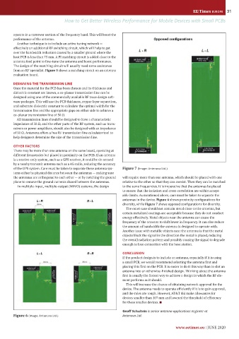
              In multiple-input, multiple-output (MIMO) systems, the design   to the same frequencies. It is imperative that the antennas be placed
                                                                 to ensure that the isolation and cross-correlation are within accept-
                                                                 able limits. As mentioned above, care must be taken to separate the
                                                                 antennas in the device. Figure 6 shows proximity configurations for
                                                                 diversity, while Figure 7 shows opposed configurations for diversity.
                                                                   The outer case should not contain metal close to the antenna, but
                                                                 certain metalized coatings are acceptable because they do not conduct
                                                                 energy effectively. Metal objects near the antenna can cause the
                                                                 frequency of the antenna to shift lower in frequency. It can also reduce
                                                                 the amount of bandwidth the antenna is designed to operate with.
                                                                 Another issue with metallic objects near the antenna is that the metal
                                                                 objects block the signal in the direction the metal is placed, reducing
                                                                 the overall radiation pattern and possibly causing the signal to degrade
                                                                 enough to lose connection with the base station.

                                                                 CONCLUSION
                                                                 If the product design is to include an antenna, especially if it is using
                                                                 a small PCB, we would recommend selecting the antenna first and
                                                                 placing this first on the PCB. It is easier to do it this way than to slot an
                                                                 antenna into an otherwise-finished design. Thinking about the antenna
                                                                 first is usually the fastest way to achieve a design in which the RF ele-
                                                                 ment performs as it should.
                                                                   This will increase the chance of obtaining network approval for the
                                                                 device. The antenna needs to operate efficiently if it is to gain approval,
                                                                 and the rules are tough. However, AT&T did make allowances for
                                                                 devices smaller than 107 mm and lowered the threshold of efficiency
                                                                 for these smaller devices. ■
                                                                 Geoff Schulteis is senior antenna applications engineer at
           Figure 6 (Image: Antenova Ltd.)                       Antenova Ltd.

                                                                                           www.eetimes.eu | JUNE 2020

